- 您现在的位置:买卖IC网 > Sheet目录3889 > PIC16F873T-04E/SO (Microchip Technology)IC MCU FLASH 4KX14 EE 28SOIC
2001 Microchip Technology Inc.
DS30292C-page 163
PIC16F87X
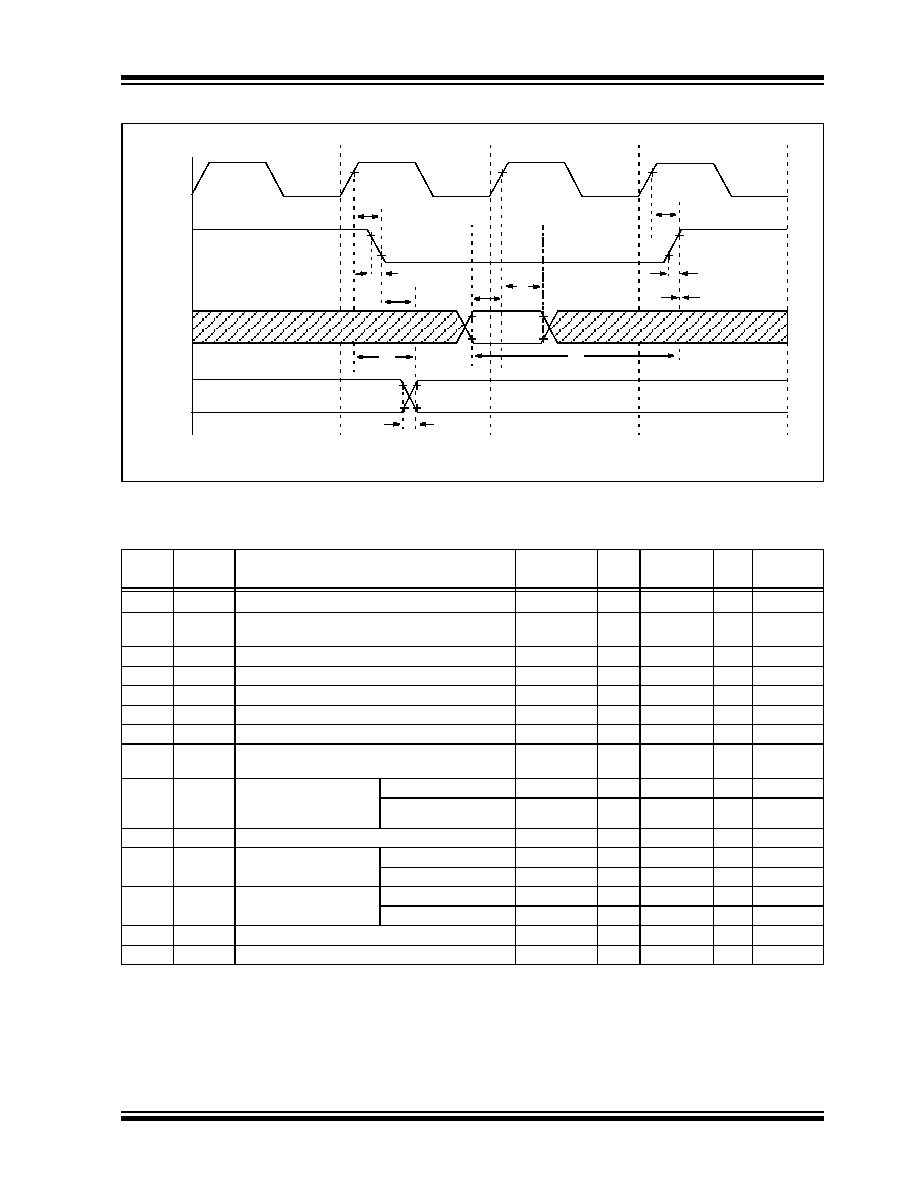
FIGURE 15-7:
CLKOUT AND I/O TIMING
TABLE 15-2:
CLKOUT AND I/O TIMING REQUIREMENTS
Note: Refer to Figure 15-5 for load conditions.
OSC1
CLKOUT
I/O Pin
(Input)
I/O Pin
(Output)
Q4
Q1
Q2
Q3
10
13
14
17
20, 21
19
18
15
11
12
16
Old Value
New Value
Param
No.
Symbol
Characteristic
Min
Typ
Max
Units Conditions
10*
TosH2ckL OSC1
↑ to CLKOUT↓
—
75
200
ns
(Note 1)
11*
TosH2ck
H
OSC1
↑ to CLKOUT↑
—
75
200
ns
(Note 1)
12*
TckR
CLKOUT rise time
—
35
100
ns
(Note 1)
13*
TckF
CLKOUT fall time
—
35
100
ns
(Note 1)
14*
TckL2ioV CLKOUT
↓ to Port out valid
——
0.5TCY + 20
ns
(Note 1)
15*
TioV2ckH Port in valid before CLKOUT
↑
TOSC + 200
——
ns
(Note 1)
16*
TckH2ioI
Port in hold after CLKOUT
↑
0
——
ns
(Note 1)
17*
TosH2ioV OSC1
↑ (Q1 cycle) to
Port out valid
—
100
255
ns
18*
TosH2ioI
OSC1
↑ (Q2 cycle) to
Port input invalid (I/O in
hold time)
Standard (F)
100
——
ns
Extended (LF)
200
——
ns
19*
TioV2osH Port input valid to OSC1
↑ (I/O in setup time)
0
——
ns
20*
TioR
Port output rise time
Standard (F)
—
10
40
ns
Extended (LF)
——
145
ns
21*
TioF
Port output fall time
Standard (F)
—
10
40
ns
Extended (LF)
——
145
ns
22*
Tinp
INT pin high or low time
TCY
——
ns
23*
Trbp
RB7:RB4 change INT high or low time
TCY
——
ns
*
These parameters are characterized but not tested.
Data in "Typ" column is at 5V, 25°C unless otherwise stated. These parameters are for design guidance only and are
not tested.
These parameters are asynchronous events not related to any internal clock edges.
Note 1: Measurements are taken in RC mode where CLKOUT output is 4 x TOSC.
发布紧急采购,3分钟左右您将得到回复。
相关PDF资料
PIC16F877T-10E/PT
IC MCU FLASH 8KX14 EE 44TQFP
22-15-3053
CONN FFC/FPC 5POS .100 RT ANG
PIC16C58BT-40/SS
IC MCU OTP 2KX12 20SSOP
PIC16C57CT-40/SO
IC MCU OTP 2KX12 28SOIC
PIC16C55AT-40/SO
IC MCU OTP 512X12 28SOIC
PIC16C56AT-40/SO
IC MCU OTP 1KX12 18SOIC
PIC16C57CT-40/SS
IC MCU OTP 2KX12 28SSOP
22-02-3053
CONN FFC/FPC 5POS .100 VERTICAL
相关代理商/技术参数
PIC16F873T-04I/SO
功能描述:8位微控制器 -MCU 7KB 192 RAM 22 I/O RoHS:否 制造商:Silicon Labs 核心:8051 处理器系列:C8051F39x 数据总线宽度:8 bit 最大时钟频率:50 MHz 程序存储器大小:16 KB 数据 RAM 大小:1 KB 片上 ADC:Yes 工作电源电压:1.8 V to 3.6 V 工作温度范围:- 40 C to + 105 C 封装 / 箱体:QFN-20 安装风格:SMD/SMT
PIC16F873T-10E/SO
功能描述:8位微控制器 -MCU 7KB 192 RAM 22 I/O RoHS:否 制造商:Silicon Labs 核心:8051 处理器系列:C8051F39x 数据总线宽度:8 bit 最大时钟频率:50 MHz 程序存储器大小:16 KB 数据 RAM 大小:1 KB 片上 ADC:Yes 工作电源电压:1.8 V to 3.6 V 工作温度范围:- 40 C to + 105 C 封装 / 箱体:QFN-20 安装风格:SMD/SMT
PIC16F873T-20/SO
功能描述:8位微控制器 -MCU 7KB 192 RAM 22 I/O RoHS:否 制造商:Silicon Labs 核心:8051 处理器系列:C8051F39x 数据总线宽度:8 bit 最大时钟频率:50 MHz 程序存储器大小:16 KB 数据 RAM 大小:1 KB 片上 ADC:Yes 工作电源电压:1.8 V to 3.6 V 工作温度范围:- 40 C to + 105 C 封装 / 箱体:QFN-20 安装风格:SMD/SMT
PIC16F873T-20I/SO
功能描述:8位微控制器 -MCU 7KB 192 RAM 22 I/O RoHS:否 制造商:Silicon Labs 核心:8051 处理器系列:C8051F39x 数据总线宽度:8 bit 最大时钟频率:50 MHz 程序存储器大小:16 KB 数据 RAM 大小:1 KB 片上 ADC:Yes 工作电源电压:1.8 V to 3.6 V 工作温度范围:- 40 C to + 105 C 封装 / 箱体:QFN-20 安装风格:SMD/SMT
PIC16F874-04/L
功能描述:8位微控制器 -MCU 7KB 192 RAM 33 I/O RoHS:否 制造商:Silicon Labs 核心:8051 处理器系列:C8051F39x 数据总线宽度:8 bit 最大时钟频率:50 MHz 程序存储器大小:16 KB 数据 RAM 大小:1 KB 片上 ADC:Yes 工作电源电压:1.8 V to 3.6 V 工作温度范围:- 40 C to + 105 C 封装 / 箱体:QFN-20 安装风格:SMD/SMT
PIC16F874-04/L
制造商:Microchip Technology Inc 功能描述:8BIT FLASH MCU SMD 16F874 PLCC44
PIC16F87404/P
制造商:Microchip Technology Inc 功能描述:MICROCONTROLLER IC
PIC16F874-04/P
功能描述:8位微控制器 -MCU 7KB 192 RAM 33 I/O RoHS:否 制造商:Silicon Labs 核心:8051 处理器系列:C8051F39x 数据总线宽度:8 bit 最大时钟频率:50 MHz 程序存储器大小:16 KB 数据 RAM 大小:1 KB 片上 ADC:Yes 工作电源电压:1.8 V to 3.6 V 工作温度范围:- 40 C to + 105 C 封装 / 箱体:QFN-20 安装风格:SMD/SMT